Now, a couple more words on the A21 topology, and the way this amp was born.
The general goal with this design was a balanced amplifier, more powerful than the A20. Having worked with power opamps for ages, I played safe in the output stage and decided to stick with National (now part of Texas Instruments) chips. During 2021 and 2022 the parts shortage was however at its peak, and LM3886, which would be a natural choice here, was out of stock for about two years, with no visible new production runs on the way. Eventually, however, I managed to source some LM4780 (now discontinued part that integrates two LM3886 in one package), so the outcome was obvious.
The A21 volume control remained principally the same as the one used in the A20 and is based on the DS1882, the so-called “digital potentiometer”, which is actually a digitally controlled resistive network. Since A21 is a balanced amplifier, one dual potentiometer chip is used for each channel.
The A21 however also required an additional input stage, to perform unbalanced-to-balanced conversion, so the output stage could give its best also with unbalanced sources. This stage required the most attention and work, and it turned out to a one of the strongest fingerprints of this amplifier.
At first, the transformers appeared ideal for such a purpose, and I discussed possible solutions with Menno van der Veen, who already designed the output coupling transformers, which perform a similar task in the S4 and S5 DACs. He could design nice input transformers too, however available toroidal cores were not small enough to fit available space. The smallest one was the one already used in the S4 and S5. In the A21, the input stage takes the central position at the PCB, so the overall layout would stretch too much.
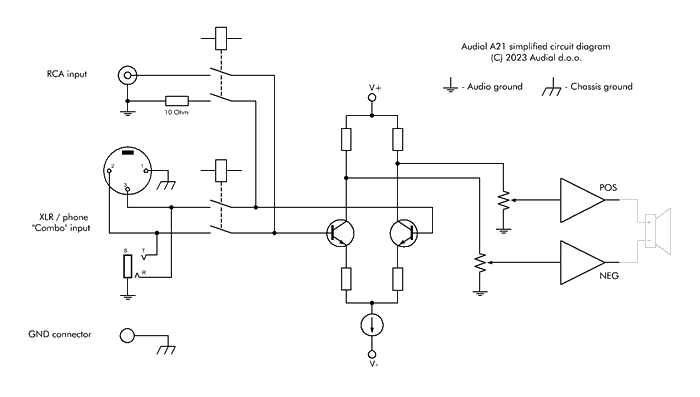
So, to do this, I worked on the active differential circuit instead, and fortunately, the result was excellent. I started by running the simulator, but most of the time I spent experimenting and designing it “by ear”, so the final circuit both sounds and measures great. As shown by the A21 simplified circuit diagram, it is based on bipolar transistors (Toshiba) and has no global feedback.
This simplified diagram also shows the input connectors and associated relay switches. Although the A21 amplifier is very simple to use and sets no special requirements regarding the rest of the system, this part may be of higher interest to its users, as it shows how the input connections and grounding are done, so they can integrate the amp into the system in the best possible way.


