
It is the holiday season, so for those still not familiar with Audial devices’ sound qualities, but with some time and will to solder, here is the idea on how to use them. The result might be both good sound, and a better understanding of audio issues.
So, here is the output stage of AYA II DAC, released back in 2007, now with details of the circuit behind the originally posted block diagram.
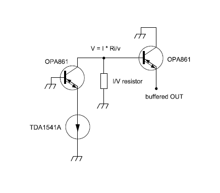
Overall, it lacks the ultimate linearity of output stages used in the Model series and Gramofone DACs – Audial latest no compromise I/V circuit distortion figure, when used with PCM1704K, went below 0.0005% (-110 dB, and no feedback, yup) – but subjectively it still fares really well. OPA861 internal circuit is for this purpose almost unbeatable diamond architecture, with the benefits of on-chip transistor matching. In fact, its sonic properties still could outperform any other published I/V circuit, as also found by some devotees earlier, when AYA II was available as an offline DIY project, namely by Elso Kwak and by Hen-Hsen Huang.
The circuit as such is intended for use with TDA1541(A), but it should be pretty easy to accommodate it to any other D/A chip. It is well-proven for its operation reliability, and this document’s data should be sufficient too. However, please be kind and note that currently we can not really support DIY endeavors, and consequently we probably won’t have time to address any questions you might have on this matter.
![]() You must be logged in to download this PDF.
You must be logged in to download this PDF.
Really a great design. I still use it in my main DAC.
Thank you for your effort and sharing. Now I can introduce my friends to this unique I/V.
You are welcome, and thank you, too.
BRs
Hi Pedja!
I want to build your I/V stage based on OPA861 and have a question. On the schematic you use two different ground-symbols, the one at the 2n2 cap is special. Does this mean that the cap should be placed close to the TDA1541? and how do you want the two gounds to be connected?
Thanx in advance
Thorsten Larsen
grounds!
Hello Thorsten.
Yes, you are correct.
These two ground symbols are not entirely standardized. Usually, the symbol you mostly see on this schematic is used for earth ground, while the symbol used for 2n2 ground is used for circuit ground. However, these two symbols are also used as a rescue in the mixed circuits schematics, to stress the difference between the digital and the analog ground.
In this case, the 2n2 ground symbol is different because this cap essentially belongs to the TDA1541(A), keeping the (highest frequencies) impedance its output “sees” low. This I/V stage itself does not really need this cap. Hence, this cap’s loop should be closed to the TDA ground, and here it means the TDA analog ground (pin 5).
Still, if you keep the overall layout (i.e. ground paths) tight, this might not be a very significant issue. Which might be an answer to your second question: ideally, these two stages should be close to each other, with a reliable, low impedance ground path in between.
BTW, please don’t try to use such a cap with a conventional opamp I/V, as the capacitance at the opamp inverting node will make it oscillate.
Regards
Thank you very much Pedja.
Thorsten
It has been about 12 years since we published this circuit (and more than 17 since I designed it for the AYA II), and very many DIY-ers have built it, and liked it, making it, among the similar AD844-based stage I published earlier, one of the de facto references in this domain. That is delightful, and surely a prize in itself, which justified the idea of posting this circuit online.
Yet, there were several “objections” about it. As these apparently came from some lack of understanding about how this circuit works, it might be the time to address them.
The first is about the (negative) feedback. The harmonic distortion of this no-feedback circuit is being compared with the circuits using it. So, for those possibly not aware of two most important associated phenomena:
1. The negative feedback is used to linearize the circuit performance, to a degree the circuit can waste its (redundant) gain. So, the negative feedback “turns the quantity into quality”. And that is how opamps normally work. If that is the goal, you easily get the harmonic distortion figure with many zeroes after the decimal point. Most audio designs, especially in the solid-state world, rely on the feedback.
2. The introduction of digital audio, however, showed all the limits of such an approach. The feedback was not apparently able to “process” high-speed signals coming out of D/A converters. Since the gain is always limited in its bandwidth, the feedback action is limited, too. In addition, because of the circuit propagation delay, the action taken by feedback could be not only ineffective but also destructive (it always comes just too late).
Essentially, with digital audio, many people did not like the sound of feedback. I certainly did not. Oftentimes, even one single transistor or single tube sounded better than the “high-performance audio” opamps.
And current feedback did not help any more, either, even if I admire highly the usual current feedback circuit structures (since my young Hiraga fan days). Finally, the OPA861 diamond “super-transistor” is one of such structures – please note that the negative feedback can also be applied to the OPA861 circuit posted here, by putting the I/V resistor between the output and the I/V chip “emitter” node (instead of between the “collector” node and the ground). I must admit that I have never tried this with OPA861, but I did it with AD844 – the result is that, the harmonic distortion figure improves, but the subjective sonic performance deteriorates, in a fundamental way. (Please see the “Distortion measurements of the AD844” at pedjarogic.com audio legacy website, and compare figures 1 and 9, to understand how easy and trivial is to improve numbers this way.)
And speaking about the opamps and feedback, my favorite piece, I/V soundwise, was OPA627, which actually uses a more classic voltage feedback. That was the only opamp that could come sonically close to no-feedback I/V circuits. The opamps however generally sounded similar, or more precisely speaking, wrong, in a similar way. Looking at their bandwidth, slew rate, phase margin, noise, etc, the opamps’ specs did not help much, nor did they point out a way to move with them. Sadly, and it was more than two decades ago when I dealt with (and abandoned) opamp I/Vs, I am not aware if anything important about opamps still changed.
Please also note that the term opamp does not denote only a specific kind of parts manufactured by the semiconductor industry. It applies to any circuit working as an opamp, be it monolithic or discrete. Furthermore, you should understand that the opamps are not the only circuits that employ feedback, and certain transistor connections can also have a feedback mechanism. For instance, the CFP, a.k.a. Sziklai pair, has a feedback action similar to the CFB (op)amps. Actually, almost any error correction topology can be regarded as some kind of local feedback. Consequently, all the feedback considerations that apply to the opamps (global) feedback may apply to such local feedback too, to a lesser or higher degree.
On the other side, just as all the other circuits I published many years ago, this OPA861 stage does NOT use feedback. Its linearity is achieved solely by the circuit itself, and not by the feedback action. As said in the original post, some I/V stages linearity can be better even without feedback, and in fact, I also published one such a discrete circuit long time ago (you can still find it also on pedjarogic.com), but taking into account the shortcomings of the public publishing, I will continue keeping the other circuits offline, for the time being.
The beauty of this one is in its simplicity and in its exceptional sound. OPA861 is one of the rare parts that can be used this way, as an I/V stage without feedback (among currently produced chips, the AD844 is probably the only other option), thus simplifying the overall effort of making one with exceptional sonic performance.
The second part is about the noise sources associated with this stage.
There are two main sources to consider here. The first is the current noise of the OPA861 “emitter” node, because it is the main OPA861 noise contributor in this application. Figures 9 and 13 of the OPA861 datasheet show the frequency content, and also this noise relation with the quiescent current, and taking into account our circuit, we can consider a general figure, in the white noise zone, as something like 3 pA/√Hz. The flicker (1/f) noise, having relatively high corner frequency, reaches ten times higher value at 100 Hz. The impedance seen by the emitter is essentially the TDA1541A output impedance, but what turns this emitter node current noise into voltage is effectively the I/V resistor. So, the emitter current noise will turn to 4.5 nV/√Hz or so, increasing to about 50 nV/√Hz at 100 Hz.
The OPA861 “base” node also contributes to the overall noise figure, both by its voltage noise of 2.4 nV/√Hz (and lower 1/f frequency than the current noise), and by its current noise of somewhat less than 2 pA/√Hz, producing, with 150 Ohm base stopper resistor, negligible 300 pV/√Hz in white noise zone, and about 2.5 nV/√Hz at 100 Hz. Since the base noise is then multiplied (i.e. in this case divided) by the ratio of the impedances in the collector and emitter – practically it is an I/V resistor, which is 1.5 kOhm, divided by the TDA1541A output impedance, which is 2.5-3 kOhm (yes, the TDA1541(A) output impedance, relatively speaking, is not very high, and it is actually one of the main constraints when you design the I/V stage without a feedback for it) – and since the summed noise is the square root of the sum of all noise sources squares, in this circuit we can roughly consider the overall base noise as a minor part (less than 20%) of the OPA861 intrinsic noise.
If needed, you can calculate the noise RMS value for the audio band, but for the record, on the spectrum analyzer with vertical axis set to dB, and where 0 dB = 2.82 V, a 50 nV/√Hz is about -155 dB, and 4.5 nV/√Hz is about 20 dB below that.
The above considerations apply to the I/V stage. In the buffer stage, the “collector” is grounded, so its noise is lower than the I/V stage noise.
If deemed to be necessary, the OPA861 datasheet includes its noise analysis model (Figure 51) and equation (Equation 8), so you can do more detailed calculations.
Speaking in relative terms, and comparing this IC both current and voltage noise to other ICs employing similar circuits, for instance to the usual CFB opamps, and which noise generation model and sources are also similar (please refer to the Analog Devices’ Tutorial MT-051), the OPA861 noise performance is mostly expected for this kind of circuit. The only objection might be the relatively high 1/f frequency of the current noise (which is a trade-off for many high-frequency parts), however the voltage noise is low.
Yet, although still not the lowest in absolute terms, this OPA861 intrinsic noise itself might not be the main contributor to the overall noise result.
A possible dominant noise contributor, in applications using their own power supplies, could be the supply itself. The OPA861 Power Supply Rejection Ratio you will find in its datasheet is given by ΔIc/ΔVs, and is 20 µA/V, typical. Since the I/V conversion in this circuit is performed by the 1.5 kOhm resistor, it becomes 30 mV/V, or 33x, or, if decibels are more descriptive, about 30 dB. This is a bit low to modern standards and should be taken into account. Say, 1 mV supply noise will translate to the audio output as something like 30 uV. If you consider the 3 V peak output level, such a 1 mV supply noise will show at the audio output at about 100 dB below the peak signal, and then you should not blame the circuit itself for it.
The supply shown in the drawing, which is also used in the AYA II and AYA 4, is adequate to provide sufficiently low noise. Its PSRR is high (the quotient of the CCS and shunt element impedances), and the shunt element intrinsic noise, although again not the best there is (it is dominated by TL431), and surely can be bettered, is fine. Besides such regulators, the AYA II and AYA 4 use Schottky diode rectifiers and common-mode RC filters.
The graphs on the PDF page 5, and more appropriate is the bottom one showing this circuit’s -60 dBFS performance, should be indicative regarding the output noise, too. Normally, now I could do more sophisticated measurements than I did 17 years ago, and go below -150 dBFS with it – both because of the better measurement A/D front-end I use now, and also because now I can use higher sampling frequencies with TDA1541A DACs (higher Fs also helps in the amplitude domain) – but the noise floor you see at these graphs are actually associated with TDA1541A performance with these signals (here you can see 1 kHz -60 dBFS measurement signal itself, it is Fs 44.1 kHz, 16-bit, triangular dither, with Fletcher-Munson curve noise shaping), and not with the output stage.
Speaking about the noise, one might also want to know what happens with resistors here. The thermal (Johnson) noise of 1.5 kOhm I/V resistor, at room temperature, is below 5 nV/√Hz, or if you consider the resistance seen by the buffer input, 2.5 kOhm thermal noise is about 6 nV/√Hz. So, since Johnson noise is white noise, and these values are low, it can be neglected. I tried different resistor types at these positions, including different carbon, tantalum, wire-wound, and metal (yikes) parts. None of them showed up on the analyzer as dominating noise factor here, so when choosing these resistors, their sonic properties should be the only criteria.
In the end, let me remind you that the noise levels I am discussing here can only be observed by modern analyzers, and are several orders of magnitude below any audibility threshold. Why this could still be important, would be another topic.
So, to sum it up. In previous years Audial released several versions of DIY AYA II and AYA 4 DACs employing this stage (the latest AYA 5 used a fully discrete output stage and supply, though), however Audial DIY items will not be available anymore, again not in the foreseeable future. So, now it is on you again to fully build such a stage yourself. Such an undertaking could be more tricky to finish that way (the layout, parts, and you will know what…), but it can be done. And it can be more fun.
And, a notice regarding the 2.2 nF caps (C405, C406), above mentioned by Thorsten. As I posted later to the Audial community forum, these caps are best omitted.
https://www.audialonline.com/community/topic/a-tweak/